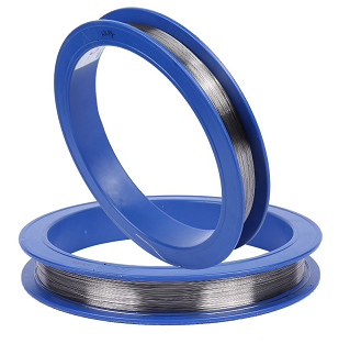
Tungsten wire is finding application as the core wire for diamond wires used in silicon wafer cutting. Tungsten wire is a fine filament primarily composed of the refractory metal tungsten (W). Characterized by a high melting point, high electrical resistivity, excellent tensile strength, and low vapor pressure, it has long been widely utilized in the lighting industry; it has now expanded into the photovoltaic sector, serving as the core wire for diamond wires used in the cutting of silicon wafers. The photovoltaic industry chain primarily comprises five key segments: polysilicon production, silicon wafer manufacturing, crystalline silicon cell production, PV module assembly, and PV power generation system integration.
The upstream segment encompasses the production of polysilicon and silicon wafers; the midstream segment covers the manufacturing of crystalline silicon cells and PV modules; and the downstream segment involves the integration and operation of PV power generation systems. Within this chain, silicon wafer cutting constitutes a pivotal process in the slicing stage. Diamond wires are employed for silicon rod cropping, silicon ingot squaring, and silicon wafer slicing; their cutting performance directly impacts both the quality of the silicon wafers and the photoelectric conversion efficiency of the resulting PV modules. As the industry advances toward thinner silicon wafers and finer-gauge diamond wires, the trend of substituting high-carbon steel wire with tungsten wire as the core material for diamond wires is becoming increasingly evident.
The production of fine tungsten wire for photovoltaic applications involves a multi-step process: First, ammonium paratungstate (APT) is roasted to yield tungsten trioxide; this is followed by two reduction reactions to produce tungsten powder. The tungsten powder is then pressed and sintered to form tungsten bars, which undergo rotary forging to create tungsten rods. These rods are subsequently drawn to produce coarse tungsten wire; finally, the coarse wire undergoes further drawing and electrolytic cleaning to yield the finished fine tungsten wire.
With the continuous advancement of silicon wafer thinning and diamond wire miniaturization, the substitution of high-carbon steel wire with tungsten wire has become an inevitable industry trend. In the future, photovoltaic silicon wafers are expected to evolve in two key directions: “larger dimensions” and “thinner profiles.” “Larger dimensions” allow for increased equipment throughput without requiring additional machinery or labor, while “thinner profiles” enhance silicon utilization efficiency and reduce raw material consumption, ultimately leading to lower production costs for photovoltaic products.
Significant room for further development remains in the field of silicon wafer thinning. In 2021, the average thickness of p-type monocrystalline silicon wafers stood at approximately 170 μm—a reduction of 5 μm compared to 2020. In 2021, the average thickness of n-type silicon wafers for TOPCon cells was 165 μm, while that for heterojunction cells was approximately 150 μm. In the future, monocrystalline silicon wafers are expected to trend toward a thickness range of 130–160 μm. According to forecasts by the photovoltaic industry association, by 2030, the thickness of monocrystalline silicon wafers will decrease significantly, reaching 110–140 μm. Furthermore, wafer thickness impacts various factors—such as cell automation, yield rates, and conversion efficiency—and must therefore meet the specific requirements of downstream cell and module manufacturing sectors.
“Fine-wiring” (reducing wire diameter) and “high-speed operation” constitute the primary development trends for diamond wire. The finer the diamond wire, the smaller the diamond micro-particles embedded in the steel wire substrate; consequently, the surface damage inflicted on the silicon wafer during the cutting process is minimized, resulting in superior wafer surface quality and improved performance across key quality metrics, such as Total Thickness Variation (TTV).
Amidst the long-term trend toward finer diamond wire substrates, tungsten wire is poised to replace high-carbon steel wire. The diameter of the cutting wire substrate and the grit size of the abrasive medium are directly correlated with silicon wafer cutting quality and material loss during cutting; specifically, smaller wire diameters and finer abrasive grits contribute to reduced material loss and lower production costs. In 2021, the diameter of diamond wire substrates ranged from 40 to 47 μm; notably, the diameter of diamond wire substrates used for cutting monocrystalline silicon wafers experienced a substantial reduction and continues on a downward trajectory.
Given the significant volatility in polysilicon prices, the shift toward finer wire substrates offers long-term strategic advantages. Beginning in late 2022, as polysilicon production capacity was gradually brought online, supply began to outstrip demand, leading to a decline in polysilicon prices and an alleviation of cost pressures on downstream wafer manufacturers. Within the context of the fine-wiring trend for diamond wire, the cyclical fluctuations in polysilicon prices will not diminish the long-term advantages of utilizing tungsten wire—rather than carbon steel wire—in photovoltaic applications. As technology continues to advance, the trend toward thinner silicon wafers in the PV industry is gaining momentum; to conserve polysilicon material and mitigate losses caused by wire breakage during the cutting process, the adoption of tungsten wire—which boasts superior physical properties—as a replacement for high-carbon steel wire has become an inevitable trend.
Driven by its slender diameter, high tensile strength (breaking force), and significant economic advantages, demand for tungsten wire is projected to experience rapid growth. Tungsten wire offers numerous advantages—including a high surface-area-to-volume ratio, high tensile strength, strong breaking force, excellent toughness, and resistance to fatigue and corrosion—and is poised to gradually replace high-carbon steel wire in the production of diamond wire. At an equivalent diameter of 40μm, tungsten wire significantly outperforms high-carbon steel wire across key metrics such as breakage rate, breaking force, resistivity, torsional performance, wire consumption, stability, and hardness; this superiority allows for savings in silicon material and extends the service life of the diamond wire.
The expanding global scale of installed photovoltaic (PV) capacity is driving growth in the diamond wire market. Amidst a global push for environmental protection, energy conservation, and emission reduction, the installed capacity of PV systems continues to expand worldwide. Notably, my country accounts for a substantial share of global solar cell production—holding a dominant position in the industry—thereby serving as a continuous catalyst for the growth of the diamond wire market. According to statistics from the China Photovoltaic Industry Association, China’s solar cell output reached approximately 318 GW in 2022—a year-on-year increase of 60.7%—accounting for 80.7% of total global production. In 2023, domestic solar cell output surged to approximately 541 GW, marking a year-on-year growth of 70.13% and setting a new record high for annual cell production.
The field of PV tungsten wire faces a dual barrier involving both technical expertise and the quality of upstream raw materials; currently, Xiamen Tungsten is the primary entity capable of achieving mass production in this sector. PV tungsten-based alloy core wires are doped with metallic elements—such as rhenium or lanthanum—to significantly enhance grit-loading capacity and uniformity by increasing the thickness of the impact-plated coating. Compared to carbon steel core wires of the same specifications, these alloy wires exhibit superior strength, lower susceptibility to brittle fracture, a higher elastic modulus, and enhanced corrosion resistance. The precise content of doping metals, as well as processing techniques such as rotary forging and wire drawing, require continuous iteration and cumulative expertise to progressively optimize the cutting performance of tungsten-wire diamond tools. FOTMA ALLOY possesses deep technical expertise and mature manufacturing processes for the production of tungsten wire. Furthermore, the trend toward finer-gauge PV tungsten wire imposes stringent quality requirements on upstream tungsten powder materials; we are uniquely positioned to guarantee a stable, vertically integrated supply of these raw materials.
Post time: Mar-15-2026