Since the 1980s, the integration density of electronic components has been increasing at a rate of more than 1.5 times per year. With the continuous improvement of integrated circuit integration, the heat generated during chip operation has increased dramatically. If heat dissipation is not timely, it will lead to thermal failure of components and significantly shorten their lifespan. Therefore, developing new electronic packaging materials with excellent thermal conductivity has become an urgent task.
01 The Prfect Combination of Diamond and Copper
Traditional electronic packaging materials mainly include three categories: ceramic materials (such as BeO, AlN), plastic materials, and metal materials (Cu, Ag, Al, etc.) and their alloys. Each of these materials has its advantages and disadvantages: ceramic materials have good matching coefficients of thermal expansion but are difficult to process; plastic materials are low-cost but have poor thermal conductivity; and metal materials have good thermal conductivity but excessively high coefficients of thermal expansion. These limitations have prompted researchers to seek better solutions.
Diamond, as the hardest known material in nature (Mohs hardness 10), also possesses extremely high thermal conductivity (200-2200 W/(m·K)). Copper, as a traditional thermally conductive material, not only boasts excellent thermal conductivity (401 W/(m·K)) but is also relatively inexpensive. Combining these advantages, diamond/copper composites have emerged and are considered the most promising high thermal conductivity electronic packaging material.
02 Key Preparation Processes Explained
Currently, the main preparation methods for diamond/copper composites include:
1) Powder Metallurgy Method: This method involves uniformly mixing diamond particles and copper powder, pressing them into shape, and then sintering. While simple and low-cost, it suffers from low density and uneven microstructure.
2) High-Temperature and High-Pressure Method: Utilizing the high-temperature and high-pressure environment provided by a six-sided press, copper is molten and fully fills the diamond mesh structure. This method produces products with excellent performance, but requires extremely sophisticated equipment, making large-scale production difficult.
3) Melt Infiltration Method: This method includes pressure infiltration and pressureless infiltration. By infiltrating molten copper into the gaps between diamond particles, high-performance composites with thermal conductivity exceeding 446 W/(m·K) can be obtained.
4) Spark Plasma Sintering (SPS): This method uses pulsed current for rapid heating and simultaneous pressure application to achieve rapid sintering. It is highly efficient but has strict requirements on the diamond volume fraction.
5) Cold Spraying: This method prepares composite materials by spraying and depositing molten metal through atomization. This technology is still in the research stage, and breakthroughs are needed in surface control and thermal conductivity.
03 The Importance of Interface Modification
Interface modification is crucial for achieving optimal performance in composite materials. Currently, two main methods are used:
1) Diamond Surface Modification: By coating the diamond surface with active elements such as Mo, Ti, W, and Cr, a carbide transition layer is formed, significantly improving the interfacial bonding state.
2) Copper Matrix Alloying: Adding appropriate amounts of active elements to the copper matrix can reduce the wetting angle and form a reinforcing phase at the interface, effectively improving thermal conductivity.
04 Future Prospects
With the continuous increase in the power density of electronic devices, traditional packaging materials are no longer sufficient to meet heat dissipation requirements. Diamond/copper composites, with their ultra-high thermal conductivity and adjustable coefficient of thermal expansion, demonstrate enormous application potential. Future research will focus on addressing key issues such as process optimization, cost control, and performance improvement to promote the widespread application of this material in the electronic packaging field.
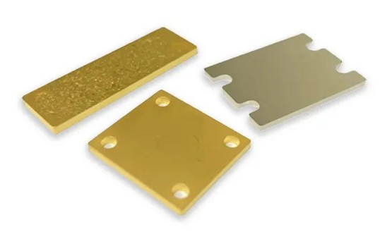
FOTMA ALLOY is a leading domestic manufacturer of diamond/copper composite materials, specializing in providing innovative thermal management solutions for high-end electronic packaging. The company possesses a complete diamond/copper composite material product system, offering end-to-end services from basic materials to precision machining. We employ internationally advanced melt infiltration processes and surface modification technologies to ensure that the composite materials possess excellent thermal conductivity (450-600 W/(m·K)) and an adjustable coefficient of thermal expansion (4.5-8.5×10⁻⁶/K), meeting the heat dissipation requirements of various application scenarios.
In terms of product supply, FOTMA ALLOY offers standard specifications of diamond/copper composite materials with thicknesses ranging from 0.5-10 mm and maximum sizes up to 500×500 mm, while also supporting customized development for customers with special size and performance requirements. The company is equipped with high-precision processing equipment and can provide a full range of processing services, including precision cutting (tolerance ±0.05mm), surface polishing (Ra≤0.1μm), coating treatment (Ni/Au, etc.), and special shape processing. To meet different application needs, we have developed a multi-specification product series with diamond content ranging from 30% to 70%, including single-crystal/polycrystalline diamond composite materials, as well as special functional products such as laser-processable models and high-insulation models.
Post time: Jan-15-2026